Datasheet4U Logo Datasheet4U.com

ADL5562 - 3.3GHz Ultralow Distortion RF/IF Differential Amplifier

General Description

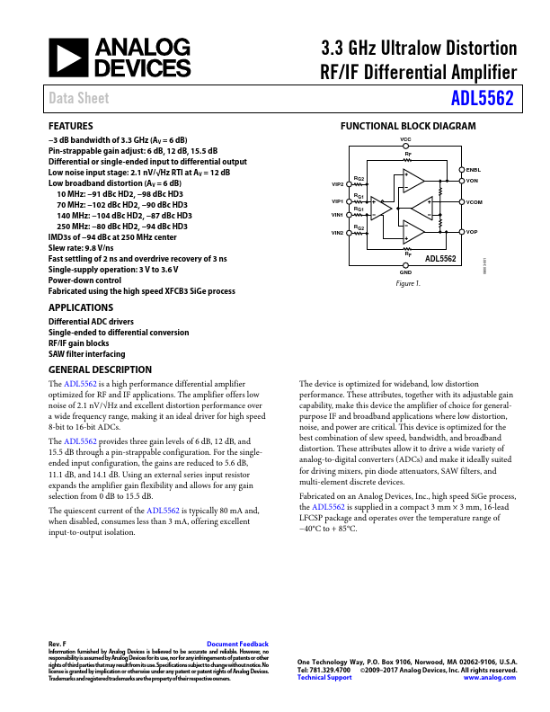
The ADL5562 is a high performance differential amplifier optimized for RF and IF applications.

The amplifier offers low noise of 2.1 nV/√Hz and excellent distortion performance over a wide frequency range, making it an ideal driver for high speed 8-bit to 16-bit ADCs.

Key Features

  • 3 dB bandwidth of 3.3 GHz (AV = 6 dB) Pin-strappable gain adjust: 6 dB, 12 dB, 15.5 dB Differential or single-ended input to differential output Low noise input stage: 2.1 nV/√Hz RTI @ AV = 12 dB Low broadband distortion (Av = 6 dB) 10 MHz:.
  • 91 dBc HD2,.
  • 98 dBc HD3 70 MHz:.
  • 102 dBc HD2,.
  • 90 dBc HD3 140 MHz:.
  • 104 dBc HD2,.
  • 84 dBc HD3 250 MHz:.
  • 98 dBc HD2,.
  • 94 dBc HD3 IMD3s of.
  • 93 dBc at 250 MHz center Slew rate: 9.8.

📥 Download Datasheet

Datasheet Details

Part number ADL5562
Manufacturer Analog Devices
File Size 558.66 KB
Description 3.3GHz Ultralow Distortion RF/IF Differential Amplifier
Datasheet download datasheet ADL5562 Datasheet

Full PDF Text Transcription for ADL5562 (Reference)

Note: Below is a high-fidelity text extraction (approx. 800 characters) for ADL5562. For precise diagrams, and layout, please refer to the original PDF.

www.DataSheet4U.com 3.3 GHz Ultralow Distortion RF/IF Differential Amplifier ADL5562 FEATURES −3 dB bandwidth of 3.3 GHz (AV = 6 dB) Pin-strappable gain adjust: 6 dB, 12 ...

View more extracted text
bandwidth of 3.3 GHz (AV = 6 dB) Pin-strappable gain adjust: 6 dB, 12 dB, 15.5 dB Differential or single-ended input to differential output Low noise input stage: 2.1 nV/√Hz RTI @ AV = 12 dB Low broadband distortion (Av = 6 dB) 10 MHz: −91 dBc HD2, −98 dBc HD3 70 MHz: −102 dBc HD2, −90 dBc HD3 140 MHz: −104 dBc HD2, −84 dBc HD3 250 MHz: −98 dBc HD2, −94 dBc HD3 IMD3s of −93 dBc at 250 MHz center Slew rate: 9.8 V/ns Fast settling and overdrive recovery of 3 ns Single-supply operation: 3 V to 3.6 V Power-down control Fabricated using the high speed XFCB3 SiGe process FUNCTIONAL BLOCK DIAGRAM VCC RF ENBL VIP2 VIP1 VIN1 VIN2 R